Using Photoshop to create a realistic PCB image
When designing PCBs that will be produced professionally (or even if you etch yourself) it is sometimes hard to get a good view of what they will look like. Most CAD programs view the design in a way that is useful during design but that is not what they will look like in the end. Some provide a view mode or 3D rendering option to get a good idea, but at least CadSoft Eagle does not. What if you want to view what your design will look like or if you just want a fancy graphic to show off your wonderful PCB? Photoshop comes to the rescue.
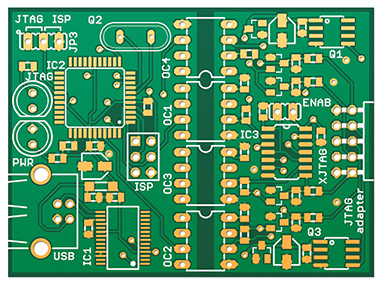
The above image is created by exporting the layers in Eagle and then processing them further with Photoshop. This article will show you how to do this.
Cleaning up
First of all, open your Eagle board and save it as a different file, in case you mess something up. If you have a lot of layout like text or size arrows outside the board then remove as much as you can:
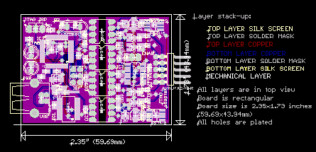
The reduced version is much smaller in this case which will make further processing easier. It isn't strictly necessary but the images you export will be a lot smaller. If your board does not have all this then just skip this step. It doesn't matter if connectors or other layout sticks out of the board, this will be cut off later.
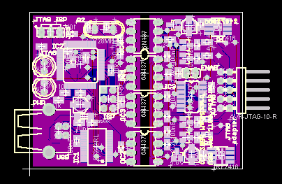
Then make sure you have a proper outline in your Dimensions layer (the white rectangular border in this case). You will need this later. Eagle has such a border by default but if you have a complex shape make sure there are outlines for all cutouts and slots.
Exporting images
The next step is exporting the layers to separate bitmap files. This can be done by switching layers on and off by hand and then exporting each but this is quite tedious. To make things easier I have a script file that does that:
Download eagle_dump.zip. Place drill-exactsize.ulp in Eagle's ULP directory, and imagedump.scr in Eagle's script directory.
Drill-exactsize.ulp is a ULP that is based on CadSoft's drill-aid.ulp and produces a layer with filled circles for every hole and drill in the board. This is needed because the default drill and hole layers do not have filled circles.
The script file imagedump.scr is simply a list of commands:
DISPLAY ALL
RATSNEST
DISPLAY None Top Pads Vias;
EXPORT IMAGE eagle_top.png MONOCHROME 600;
SET FILL_LAYER tStop 1;
SET FILL_LAYER bStop 1;
DISPLAY None Bottom Pads Vias;
EXPORT IMAGE eagle_bottom.png MONOCHROME 600;
DISPLAY None tStop;
EXPORT IMAGE eagle_top_mask.png MONOCHROME 600;
DISPLAY None bStop;
EXPORT IMAGE eagle_bottom_mask.png MONOCHROME 600;
DISPLAY None tPlace -tOrigins tNames -tValues -tDocu;
EXPORT IMAGE eagle_top_silk.png MONOCHROME 600;
DISPLAY None bPlace -bOrigins bNames -bValues -bDocu;
EXPORT IMAGE eagle_bottom_silk.png MONOCHROME 600;
SET FILL_LAYER drillImage 1;
DISPLAY None drillImage
EXPORT IMAGE eagle_drill.png MONOCHROME 600;
DISPLAY None Dimension;
EXPORT IMAGE eagle_outline.png MONOCHROME 600;
The drill-exactsize ULP is run first, this produces the new drillImage layer. Besides some other settings you can see pairs of DISPLAY and EXPORT commands. The DISPLAY commands select which layers to show, the EXPORT command right after it saves the layers that are displayed to a PNG file. 600 is the resolution, which is a good number to work with but you can change it something else if you like. This script is also the place to select which layers to use for the different PCB layers, just add them to the DISPLAY commands. A minus sign '-' in front of a layer means hiding it. Some layers (like tPlace) automatically also display other layers (such as tOrigins, tNames, etc.) which then have to be hidden explicitly.
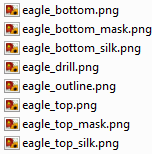
Now, just run imagedump.scr from Eagle and it will write a set of files. By default Eagle writes these files to your active project directory. Note that this may not be the same directory as your board as saved in, if you can't find your files look in the main window of Eagle and find the active project (with the green bullet right next to it). This is the directory where it saved the files. You should have got these eight files:
Photoshop
Next start photoshop, and open the eagle_outline.png file. It should display as a black image with a very thin white board outline. If you cannot see the outline try zooming in or out:
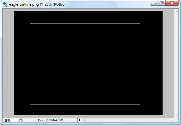
The image needs to be converted from Indexed to RGB mode. Click image, mode, RGB color. The title of the image will now say 'RGB/8'.
With the magic wand tool, select the inside of the outline, so that the selection is equal to your actual PCB area. If you have any holes in the PCB, use the rectangular marquee tool with shift pressed to select around them and add them to the selection.
Create a new layer named base, with your selection still active. Select black as the foreground color (just press d) and fill the selection with alt+backspace. Then remove the background layer with the original outline image, and you should have your board shape in black with the rest transparent:
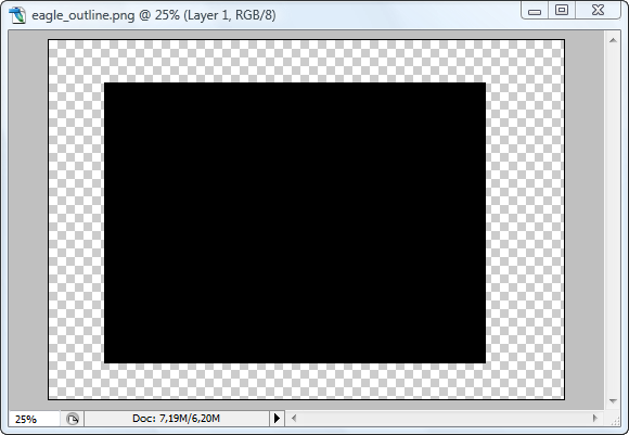
In the layers palette, lock the layer transparency with this button:
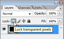
Then hide this layer for now, and save the file.
Adding layers
The following steps need to be repeated for the remaining seven files. Two files need an additional action. Each file will end up in its own layer. The steps are as follows:
First open a file, here eagle_top_copper is taken as an example. Select everything in the file (ctrl+A), copy it to your clipboard (ctrl+C) and close the file.
Go back to your PCB image and add a new layer. Use a name similar to the original file (such as 'top copper' for this example). Select all (ctrl+A), which selects nothing and then press Q to enter quick mask mode. Now paste your clipboard image, which should look similar to this:
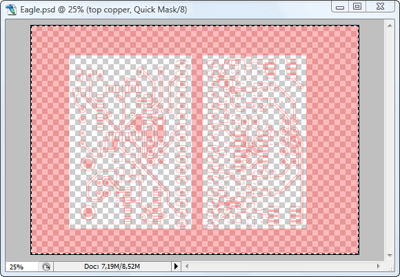
Press Q again to go back to normal mode, your image now appears in the form of your selection. Make sure you still have black as the foreground color and fill the selection with alt+backspace. Deselect all (ctrl+B) and your image now is black with a transparent background.
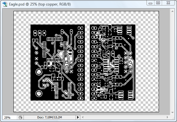
Finally lock the transparency of the layer, as you have done earlier with the base layer.
The above steps need to be done for every PNG file (except outline which was already done) so that each ends up in transparent and black in its own layer. Note: eagle_top_mask and eagle_bottom_mask are negative images, for these you will have to invert the selection (ctrl+shift+I) before filling it with alt+backspace. The mask layers should be black with only the pads etc. transparent.
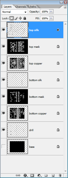
When all layers are done give them proper names if you haven't done so already and order them like I have done below. Also make sure all layers have their transparency locked!
Drill holes and outline
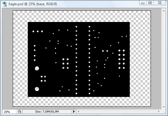
Some layers may have the drill holes filled or have parts outside the board outline. To fix this, hide all layers except for the drill and base layers. Hold ctrl and click on the thumbnail of the drill layer in the layers palette. This should select all drill holes. Delete the drills layer and activate the base layer with the selection still active. Pressing delete will cut out all the drill holes of this layer and leaves the final physical board shape:
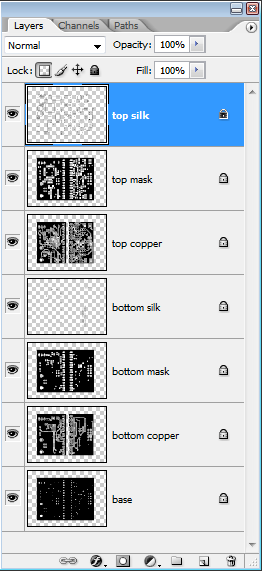
Make all layers visible, then hold ctrl again and now click on the thumbnail of the base layer. The base layer shape will transform in a selection. Invert this selection with ctrl+shift+I. For each other layer, keep the selection active and activate the layer. Press delete to remove everything that is outside the board or inside a drill hole. After you are done with this all layers should have the correct shape:
Adding color
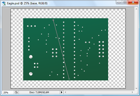
For the color of the layers I usually use some gradients. It is useful to save these gradients as presets as you need them multiple times and maybe in the future for other boards. The colors can of course be customized to reflect the final design. This example will show a green coated PCB with gold plated pads. I will start with the top side, the bottom side can be done in exactly the same way.
First create a gradient with two dark shades of green for the PCB base.

Show the base layer and hide all other layers. Use the gradient fill tool to fill it as such. You don't need to select anything, if you set the transparency lock the gradient will only fill the black areas automatically.
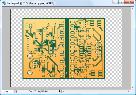
For the gold plating I use some yellow/orange gradient:

Show the top copper layer and fill it again:
Finally the solder mask, which is also green but a lighter shade than the base. Just experiment a bit with these colors.

Show the top mask layer and fill it as well.
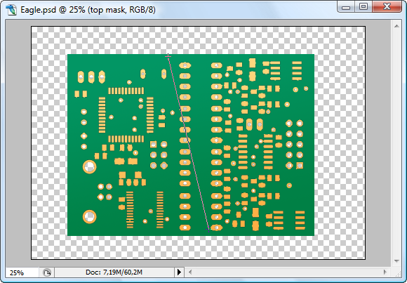
You will notice that the mask completely covers the trace pattern, to fix this the mask will be shown only where copper is present. This is not how it is in reality but it is easier to work with and looks correct in the end.
Hold ctrl and click on the thumbnail of the top copper layer to select all copper. Invert the selection with ctrl+shift+I, activate the top mask layer and press delete. The mask will now show correctly:

Adding highlights and shades
The image still looks flat, so we need to add a bit of bevel to the layers. Add a bevel and emboss effect to the copper layer and use something like these settings. But again, experiment with this!
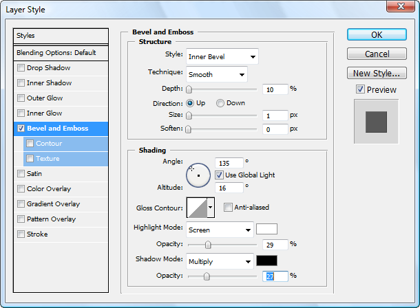
Do the same with the top mask layer and it will look a lot better already:
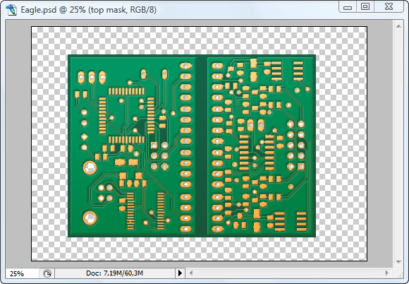
To add the silkscreen, show the top silk layer. To turn the silkscreen white, select white as the foreground color (D, X) with the layer active and press alt+backspace to fill it. Because silkscreen has some thickness in real life as well, you can add a small amount of bevel to it similar to the copper and mask layers until you get something like this:
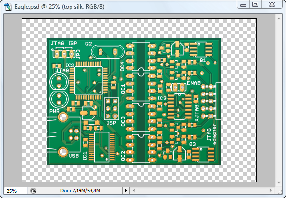
The above two sections can be repeated for the bottom layers. These are mirrored but just work with them as if they were correct. This will be fixed later:
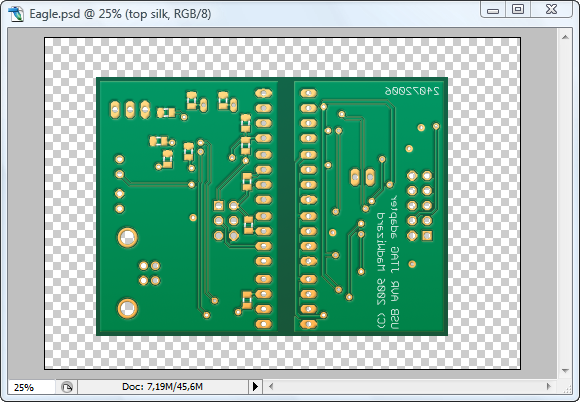
Extracting top and bottom
If you have finished the top and bottom you can combine the layers with the following steps:
Show the base layer and three top layers, hide all bottom layers. Make sure you have one of the visible layers as your active layer. Select all (ctrl+A) and copy all layers merged (ctrl+shift+C). Create a new document (ctrl+N), usually the size is already matched to your clipboard image size but adjust it so that at least the top and bottom images fit in the new image and you still have a bit of headroom for the shadows. Paste the clipboard as a new layer in your new file.
Go back to your original file. Save the file if you haven't done so already, then flip the canvas horizontally with image, rotate canvas, flip canvas horizontally. This needs to be done here because flipping the canvas later would also flip the effects and make the bevel lighting incorrect. Now show the three bottom layers and the base layer and hide the top layers. Again make sure you have a visible layer active, select all (ctrl+A), copy merged (ctrl+shift+C). Paste this image in the new image next to the top image. You can close the original file without saving if you don't want the image saved flipped horizontally. Make sure you have saved right before the flip of course.
You should now have the top and bottom as single layers in a new file. Add a little shadow effect to both and you are done:
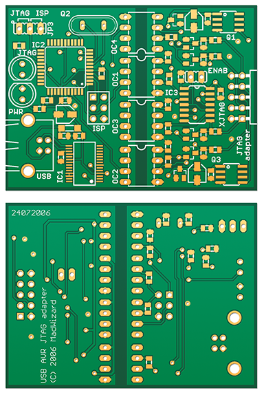
Hopefully you can now make these images yourself. You can always try out other colors or techniques now that you know the basics.